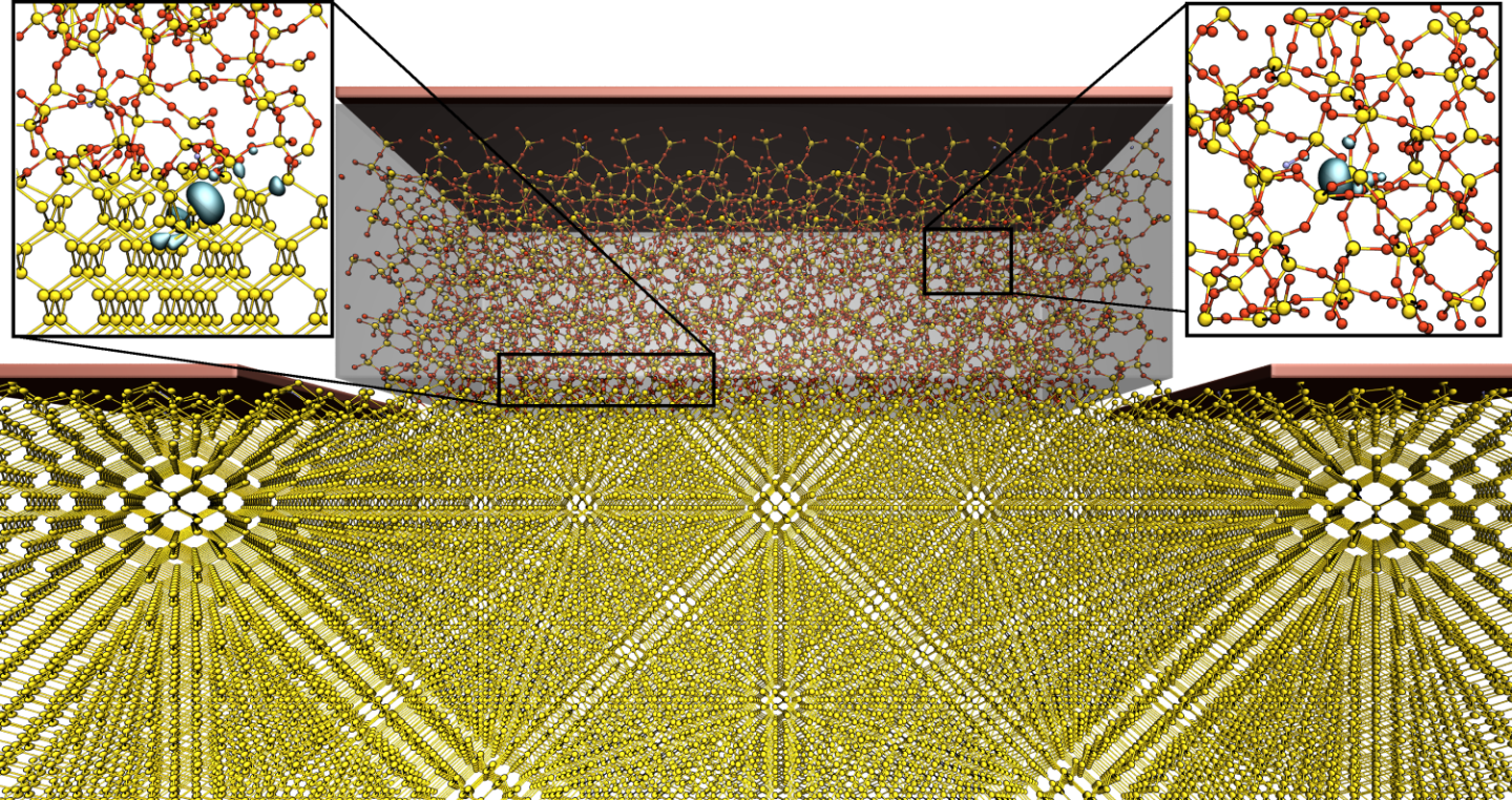
The quality of modern ultra-scaled electronic devices is substantially influenced by processing conditions. In particular, their variability and reliability is impacted by electrically active defects at the channel-oxide interface and within the oxide layer. The formation of these intrinsic defects, however, is inevitably linked to various manufacturing steps like chemical oxidation, forming gas anneal, plasma nitridation and atomic layer deposition of high-k materials.
To break new grounds, this WP focuses on the formation and implication of different defect types at the process level. State-of-the-art multiscale atomistic simulation approaches, ranging from molecular dynamics to density functional theory, are employed to identify the relevant reaction kinetics of defect formation and transformation within the important low-temperature processing steps.
In that connection, this WP forms a close synergy with the other WPs, benefiting from the experimental input to improve the atomistic models, and on the other hand, providing the theoretically assessed reaction dynamics as inputs for subsequent simulation approaches, such as the developed kinetic Monte Carlo methods. Ultimately, the outcome can be seen as a next step towards predictive modeling of device reliability issues based on fundamental atomistic kinetics which occur at the processing level.
WP5 coordinator: Tibor Grasser, TU Wien